India's No.1 PU & Degree With Integrated IAS & IPS(UPSC/PSC) Training College.

Semicon 2.0 Expands India’s Chip Support Plan
Semicon 2.0 Expands India’s Semiconductor Support Framework
Why in the News ?
The Union Government has notified Semicon 2.0, reducing financial support for eligible silicon fabrication projects from 50% to 40% while expanding assistance for semiconductor packaging, display fabrication, equipment, materials, chip design, research and talent development.
Key Changes Under Semicon 2.0
- Under Semicon 1.0, launched in 2022, eligible silicon fabrication units could receive government support equivalent to 50% of project cost.
- Semicon 2.0 reduces this support to 40% of eligible capital expenditure.
- IT and Electronics Minister Ashwini Vaishnaw termed the revised assistance “globally competitive”, arguing that growing investor confidence in India justified a lower subsidy.
- The renewed scheme has a total financial outlay of ₹1.27 lakh crore.
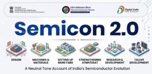
- It is organised around six major pillars, covering chip design, semiconductor equipment and materials, expanded fabs, advanced packaging, R&D and talent development.
- Support for the semiconductor ecosystem has also been broadened beyond conventional fabrication facilities.
Boosting Innovation, Design and Domestic Capability
- Semicon 2.0 seeks to strengthen India’s semiconductor value chain rather than focusing exclusively on fabrication.
- Commercial chip-design startups and MSMEs can receive seed funding of up to ₹15 crore.
- Larger eligible companies may access royalty financing or equity co-investment, while equity support will also be available for smaller innovators.
- The expanded framework aims to promote domestic manufacturing, reduce dependence on imported semiconductor inputs and develop indigenous technological capabilities.
- Support for R&D and talent development is intended to address skill shortages and strengthen India’s semiconductor workforce.
- The government believes India has moved from being viewed cautiously by global semiconductor companies in 2022 to becoming a more credible destination for long-term semiconductor investment.
- The broader objective is to establish a resilient end-to-end semiconductor ecosystem, spanning design, manufacturing, packaging, equipment, materials and skilled manpower.
About Semiconductor Ecosystem and Technology:● Semiconductor fabs manufacture integrated circuits on silicon wafers and form the core of the chip-production ecosystem. ● Semicon 2.0 provides 35% support for advanced packaging, including 2.5D and 3D packaging, wafer-level chip-scale packaging and heterogeneous integration. ● Legacy packaging projects will receive 25% support. ● Dedicated assistance has been introduced for display fabrication, covering OLED, Micro LED and LCD technologies. ● OLED and LCD projects involving at least ₹10,000 crore investment will receive 35% support, while Micro LED projects require at least ₹1,500 crore and receive the same support. ● The scheme also covers semiconductor equipment, sub-assemblies, components, wafers, photomasks, photoresists, substrates, chemicals and industrial gases. ● Equipment manufacturers can receive a separate Production-Linked Incentive (PLI) based on components procured from domestic manufacturers. |