
THE NEED TO OVERHAUL A SEMICONDUCTOR SCHEME
Relevance: GS 2 – Government policies and interventions for development in various sectors and issues arising out of their design and implementation.
Why in the News?
- Appraisal upcoming for the semiconductor Design-Linked Incentive (DLI) scheme.
- Only seven start-ups have been approved since its announcement, significantly below the targeted support for 100 start-ups over a five-year period.
- Thus, Mid-term appraisal is imminent, providing an opportunity for policymakers to evaluate and potentially revamp the scheme.
- Also, the $10 billion Semicon India Program has yielded mixed results.
Three primary goals of India’s semiconductor strategy
- Reduce dependence on semiconductor imports, with a focus on strategic and emerging sectors, such as defence applications and Artificial Intelligence development.
- Build supply chain resilience by integrating into the global semiconductor value chain (GVC).
- Capitalize on India’s comparative advantage, leveraging the presence of design houses for major global semiconductor industry players and the integral role of Indian chip design engineers in the semiconductor GVC.
Strategic Considerations for Policymakers
- Evaluate the reasons behind the limited approval of start-ups.
- Consider adjustments to enhance the scheme’s effectiveness in fostering semiconductor innovation and entrepreneurship.
- Revision of policies may be necessary to align with the original objectives and ensure sustained support for semiconductor start-ups.
- Engage with stakeholders to gather insights on challenges faced by start-ups in the semiconductor sector.
- Foster collaboration between policymakers, industry experts, and start-ups to refine and optimize the DLI scheme.
- Consider industry feedback to tailor the scheme for maximum impact and sustainability.
Strategic Goals for Semiconductor Powerhouse Status:
- Establishing India as a semiconductor powerhouse through strategic goals.
- Recognizing the limited resources and the need for prioritization in industrial policy.
- Prioritizing goals to ensure disproportionate benefits from investments.
- Acknowledging the importance of maximizing outcomes given resource constraints.
- Stimulating Design Ecosystem:
- Recognizing the less capital-intensive nature of stimulating the design ecosystem compared to foundry and assembly stages in the semiconductor Global Value Chain (GVC).
- Emphasising the potential for strong forward linkages by bolstering the design stage. Highlighting the opportunity to establish robust forward linkages to a burgeoning fabrication and assembly industry in India.
- Stating the potential benefits of focusing on the design ecosystem for long-term industry growth.
- Policy Scrutiny Discrepancy:
- Observing a lack of policy scrutiny regarding the Design-Linked Incentive (DLI) scheme’s outcomes.
- Noting the contrast with the swift revisions made to Production-Linked Incentive schemes for foundries and assembly stages.
- Pointing out the disparity in the level of attention given to different components of the semiconductor value chain.
- Need for Equitable Policy Attention:
- Addressing the anomaly in policy attention between different stages of the semiconductor industry.
- Emphasising the importance of equitable scrutiny and adjustments to ensure a balanced and effective semiconductor strategy.
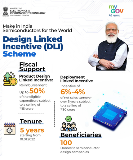
Issues with the DLI Scheme
The DLI Scheme focuses on providing access to design infrastructure, particularly electronic design automation (EDA) tools and offers financial subsidies for various stages of the chip design process. But various issues came across during the prima facie assessment of the scheme.
- Mandatory Domestic Status Requirement:
- DLI scheme mandates beneficiary start-ups to maintain domestic status for at least three years after receiving incentives.
- Imposes a significant barrier by restricting the ability to raise more than 50% of requisite capital via foreign direct investment.
- Semiconductor Design Startup Funding:
- Long-term payoff in semiconductor R&D poses challenges in the funding landscape.
- Challenging funding environment despite promising IP and business potential.
- Risk Aversion of Domestic Investors:
- Lack of success stories in hardware product startups reduces the risk appetite of domestic investors.
- Capital requirements and absence of a mature startup funding ecosystem contribute to the challenge.
- Equity Financing and Foreign Funds:
- Shortfall in investment for DLI beneficiary start-ups could be mitigated by equity financing with foreign funds.
- Challenges arise due to scheme’s restrictions on ownership, limiting the infusion of foreign capital.
- Modest Incentives and Funding Trade-offs:
- Relatively modest incentives under the DLI scheme, capped at ₹15 Crore for Product DLI and ₹30 Crore for Deployment Linked Incentive per application.
- Start-ups may find the trade-off unappealing, risking crucial long-term funding opportunities.
- Delinking Ownership for Start-up-Friendly Guidelines:
- Advocating for delinking ownership from semiconductor design development.
- Suggesting more start-up-friendly investment guidelines to attract foreign funds and boost financial stability.
- Focus on Semiconductor Design Capabilities:
- Proposing a shift in the primary aim of the DLI scheme towards cultivating semiconductor design capabilities in India.
- Emphasizing that home-grown IP will evolve organically as local talent fosters the creation of indigenous companies over time.
- Revised Scheme Objectives:
- Calling for a revision of the DLI scheme to focus on facilitating design capabilities for a variety of chips within the country.
- Suggesting that the entity engaging in the design development process needs to be registered in India, aligning with the government’s recent statement.
- Government’s Direction and Financial Enhancement:
- Acknowledging the government’s recent statement emphasizing “India-designed chip.”
- Urging a substantial enhancement of the financial outlay of the DLI scheme to support the policy shift towards promoting indigenous semiconductor design capabilities.
Nodal Agency Role
- The role of the Centre for Development of Advanced Computing (C-DAC) as the nodal agency for appraising DLI scheme proposals warrants reconsideration.
- Clear concerns about potential conflicts of interest arise due to C-DAC’s dual role as a market player in the Indian chip design sector.
- Suggesting a reevaluation of the implementing and regulating role of C-DAC.
- Alternative Implementing Agency – SFAL as Blueprint:
- Proposing the Semiconductor Fabless Accelerator Lab (SFAL) under the Karnataka government as a suitable blueprint for an implementing agency for the DLI scheme.
- SFAL’s successful model with specific partnerships involving the Indian Electronics and Semiconductor Association, EDA vendors, IP, and testing companies.
- Similar agency under India Semiconductor Mission: Recommending the establishment of a similar agency under the India Semiconductor Mission.
- This agency could emulate SFAL’s approach, providing start-ups access to mentors, industry networks, and financial institutions, alongside financial incentives disbursed under the DLI scheme.
- Expanded Focus for DLI Scheme:
- Proposing a recalibrated DLI scheme with an expanded focus to attract a broader range of semiconductor design start-ups.
- The revamped scheme should not be limited to those ready for volume production, fostering support for start-ups overcoming initial hurdles in developing design ideas.
- Comprehensive Support Ecosystem:
- Envisioning the new agency as a comprehensive support ecosystem, inspiring a network of mentors, industry connections, and financial backing for affiliated start-ups.
- Aiming to create an environment conducive to fostering innovation and overcoming challenges in the semiconductor design sector.
- Tolerance for Exploration and Risk:
- Emphasizing the need for a recalibrated policy focused on chip design, led by a capable institution.
- Advocating for a mindset that tolerates a certain failure rate, treating beneficiary start-ups as exploratory risk-taking vehicles to establish India’s foothold in the high-tech semiconductor sector.
Source:
Mains question
Examine the challenges in India’s semiconductor industry, focusing on the Design-Linked Incentive (DLI) scheme. Discuss potential reforms, including the role of implementing agencies and the need for a broader focus. (250 words)